
|
| |
|
Строительный блокнот Introduction to electronics Tramislor wavefonns theinterviil < ( < C, the diode remains forward-biased, and hence the transistor voltage is V. At time f = f[, the stored charge in the vicinity of the ;Г or p--i junction is exhausted. This junction becomes reverse-biased, and begins to block voltage. During theinterval r, < /< /j, the diode voltage decreases to -V. Some negative diode current continues to flow, removing any remaining stored minority charge as well as charging the depletion layer capacitance. At time / = fj. this current is essentially zero, and the diode operates in steady state under reverse-biased conditions. Diodes in which the interval length (t - (;) is short compared to (/ - (() are called abrupt-recovery or snappy diodes. Soft recovery diodes exhibit larger values of ((; - ([VCfi - t). When significant package and/or stray inductance is present in series with thediode, ringing of the depletion region capacitance with the package and stray inductances may be observed. If severe, this ringing can cause excess rever.se voltage that leads to device failure. External R-C snubber circuits are sometimes necessary for reliable operation. The reverse-recovery characteristics of soft recovery diodes are intended to exhibit less ringing and voltage overshoot. Snubbing of die.se diodes can be reduced or eliminated. The instantaneous power Рд(Г) dissipated in the transistor is also sketched in Fig. 4.51. The energy lost during the turn-on transition is
Diode waveforms (4.9) Helling liiLilsiuon For an abrupt-recovery diode in which (tj-j) -* (fj -( ), this integral can be evaluated in a simple manner. The transistor voltage v{t) is then equal to for essentially the entire diode recovery interval. Inaddition, = i - \g. Equation (4.9) then becomes jwiichir iTiiniiiun f-ij.i)]di 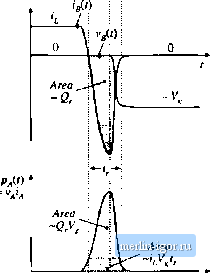 (4.10) Fin. 4.51 TransJatoi-turii-oii transition waveforms for the circuit of Fig. 4,50. where the recovered charge is defined as the integral of the diode current - igif) over theinterval < f < fj. Hence, the diode reverse recovery prticess leads directly to switching loss Wjf. This is often the largest single component of switching loss in a conventional switching converter. It can be reduced by use of faster diodes, designed for minimization of stored minority charge. Swuch ReaKzalion Ky. 4.52 Tlie energy swretl in llie semiconductor out)Ut capacitances is last during ilie transistor turn-on tiansition. 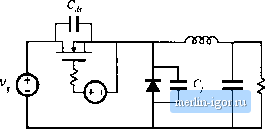 4.3.3 D vlc Capacitances, and Leakage, Package, and Stray Inductances Reactive elements can also lead to switching loss. Capacitances that are effectively in parallel with switching elements are shorted out when the switch turns on, and any energy stored in the capacitance is lost. The capacitances are charged without energy loss when the switching elements turn off, and the transistorturn-offloss Wjj computed in Eq. (4.7) may be reduced. Likewise, inductances that are effectively in series with a switching element lose their stored energy when the switch turns off. Hence, series inductances lead to additional switching loss at turn-off, but can reduce the transistor turn-on loss. The stored energies of the reactive elements can be summed to find the total energy loss per switching period due to these mechanisms. For linear capacitors and inductors, the stored energy is [ ;ii2iti \v = S i/./; intUiuliwi; (4,11) A common source of this type of switching loss is the output capacitances of the semiconductor switching devices. The depletion layers of reverse-biased semiconductor devices exhibit capacitance which stores energy. When the transisttu turns on, this stored energy is dissipated by the transistor. For example, in the buck converter of Fig. 4.52, the MOSFET exhibits drain-to-source capacitance C and the reverse-biased diode exhibits junctioncapacitance Cj, During the switching transitions these two capacitances are effectively in parallel, since the dc source V is effectively a short-circuit at high frequency. To the extent that the capacitances are linear, the energy lost when the MOSFET turns on is (4.12) Typically, this type of switching loss is significant at voltage levels above 1(Ю V. The MOSFET gate drive circuit, which must chaige and discharge the MOSFET gate capacitances, also exhibits this type of loss. As noted in Section 4.2.2, the incremental drain-to-source capacitance C . of the power MOSFET is a strong function of the drain-to-source voltage Vj. C,J(,J) follows an approximate inverse-square-root dependence of v as given by Eq. (4.5). The energy stored in C at v = K,. is (4.13) where = Q Cv,;,) dviJdi is the current in t ,. Substitution of Eq. (4.5) into (4.13) yields (4.14) This energy is lost each time the MOSFET switches on. From the standpoint of switching loss, the drain-to-source capacitance is equivalent to a linear capacitance having the value C JVus) The Schottky diode is essentially a majority-carrier device, which does not exhibit a reverse-recovery transient such as in Fig. 4.51. Reverse-biased Schottky diodes do exhibit significant junction capacitance, however, which can be modeled with a parallel capacitor Cj as in Fig. 4.52, and which leads toenergy loss at the transistor turn-on transititm. Common sources of series inductance are transformer leakage inductances in isolated converters (discussed in Chapter 6), as well as the inductances of interconnections and of semiconductor device packages. In addition to generating switching loss, these elements can lead to excessive peak voltage stress during the transistor turn-off transition, interconnection and package inductances can lead to significant switching loss in high-current applications, and leakage inductance is an important source of switching loss in many trdnsformer-isolated converters. Diode stored minority charge can induce switching loss in the (nonideal) converter reactive elements. As an example, consider the circuit of Fig. 4.53, containing an ideal voltage source an inductor L, a capacitor С (which may represent the diode junction capacitance, or the junction capacitance in parallel with an external capacitor), and a silicon diode. The diode switching processes of many converters can be modeled by a circuit of this form. Many rectifiercircuits ctmtaining SCRs exhibit similar waveforms. The voltage source produces the rectangular waveform V;(r) illustrated in Fig, 4.54. This voltage is initially positive, causing the diode to become forward-biased and the inductor current ifit) to increase linearly with slope V/L. Since the current is increasing, the stored minority charge inside the diode also increases. At time / = f the source voltage v.(t) becomes negative, and the inductor current decreases with slope dij/dt = - Vj/L. The diode stored charge also decreases, but at a slower rate that depends not only on but also on the minority carrier recombination lifetime of the silicon material in thediode. Hence, attime ; = /;, when i,(() reaches zero, some stored minority charge remains in the diode. So the diode continues to be forward-biased, and the inductor current continues to decrease with the same slope. The negative current for ( > constitutes a reverse diode current, which actively removes diode stored charge. At some time later, t = tj, the diode stored charge in the vicinity of the diodejunction becomes zero, and the diodejunction becomes reverse-biased. The inductor current is now negative, and must How through the capacitor. The inductor and capacitor then form a series resonant circuit, which rings with decaying sinusoidal waveforms as shown. This ringing is eventually damped out by the parasitic loss elements of the circuit, such as the inductor winding resistance, inductorcore loss, and capacitor equivalent series resistance. The diode recovered charge induces loss in this circuit. During the interval < r < the minority stored charge recovered from the diode is 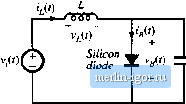 Fig. 4,53 A circuit In whieh (he diode stored thnrge induces ringing, and uiiimacely switching 10.Ч.Ч, in (nonideal) reactive elements. a=- ii(t)dt (4,15) |