
|
| |
|
Строительный блокнот Introduction to electronics Table 5,1 CCM-DCM mode boundaries for the buek, boost, and buck-boysl eonvertcj s Converter min (/i ,) Buck Boost (1-d) D{1 - Df Buck-boost (1 - of- (\-Dyr, 2L 2 Г. tance R is defined as tlie ratio of the dc output voltage to the dc load current: R = V/1. This effective load resistance is then used in the above equations. A similar mode boundary analysis can be performed for other converters. The boost converter is analyzed in Section 5.3, while analysis of the buck-boost converter is left as a homework problem. The results are listed in Table 5.1, for the three basic dc-dc converters. In each case, the dimensionless parameter is defined as К - lUKi]., and the mode boundary is given by K>K jU) or R<R,JP) forCCM <A: (D) or R>R,(P) for DCM (5.8) 5.2 ANALYSIS t)F THE CONVERSION RATIO M(D, K) With a few modifications, the same techniques and approximations developed in Chapter 2 for the steady-state analysis of the continuous conduction mode may be applied to the discontinuous conduction mode. (a) Inductor volt-second balance. The dc component of the voltage applied to an inductor mast be zero: (5.J) (b) Capacitor charge balance. The dc component of curreiu applied to a capacilor must be zero: (,-,) = \-,(,)Л = и <5.I0) These principles must be Urue for any circuit that operates in steady state, regardless of the operating mode. (c) The linear ripple approximation. Care must he used when employing the linear ripple approximation in the discentinttoas coitduction mode. ti Output capacitor voltage ripple. Regardless of the operatiitg mode, it is required that the output voltage ripple be small. Hence, for a well-designed converter operating in the discontinuous conduction mode, the peak output voltage ripple Av shottid be much smaller in magnitude than the otttpttt vohage dc component V. So the linear ripple approximatioit аррИея to the output voltage waveform: (5.11) {ii) tndnaor airrenr ripple. By definition, the inductor current ripple is not small iii the discoiitinaons conduction mode, trdeed, Eq. (5.3) slates that the inductor current ripple Ai is greater in magnitude than the dc component J. So neglecting the inductor current ripple leads to inaccurate results. In other converters, several inductor currents, or a capacitor voltage, may contain large switching ripple whicti should noi be negtected. The equations necessary for solution of the vtdtage conversion ratio can be obt;uned by invoking volt-second balance for each inducttjr voltage, and charge balance for each capacittjr current, in the network. The switching ripple is ignored in the output capacitor voltage, but the inductor current switching ripple must be accounted for in this buck converter example. Let us analyze the conversion ratio M = V/V of the buck converter of Eq. (5.1). When the transistor conducts, forO< ( <0Г, the converter circuit reduces to the network of Fig. 5.7(a). The inductor voltage and capacitor current are given by Vi(f) = V,-KO (5.12) By making the linear ripple approximation, to igntjre the output capacitor voltage ripple, one obtains Fig. 5.7 Buck converter circuits for operation In the (iiscontinuous conduction mode: (a) duruig suhinterval 1, (h) during subiutefval 2, (c) during subinterval 3, 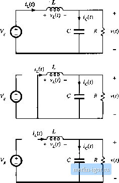 (5.13) itr) = /,(0- Note that the inductor currenl ripple has not been ignored. The diode conducts during subinterval 2, DjTj < < (L\ -i- Щ)Т- The circuit then reduces to Fig. 5.7(b). The inductor voltage and capacitor current are given by icO-hm--f By neglecting the ripple in the output capacitor voltage, one obtains v,(r) = -V (5.15) The diode becomes reverse-biased at time T = iD + DyT. The circuit is then as shown in Fig. 5.7(c), with both transistor and diode in the off state. The inductor voltage and inductor current are both zero for the remainder of the switching period (Д; + D-JT < < The networic equations for the third subinterval are given by y, = 0, =0 icit)i,{t)- Note that the inductor current is constant and equal to zero during the third subinterval, and therefore the inductor voltage must also be zero in accordance with the relationship \j(t) = Ldif{t)!dt. In practice, parasitic ringing is observed during this subinterval. This ringing occurs owing to the resonant circuit formed by the inductor and the semiconductor device capacitances, and typically has little influence on the converter steady-state properties. Again ignoring the output capacitor voltage ripple, one obtains Equations (5.13), (5.15), and (5.17) can now be used to plot the inductor voltage waveform as in Fig. 5.S. According to the principle of inductor volt-second balance, the dc component of this waveform must be zero. Since the waveform is rectangular, its dc component (or average value) is easily evaluated: {.lit)) = V, - V) -H Dj[- f )- Лз(п) = 0 (5.IS) Solution for the output voltage yields y~Y 1 (5.19) The transistor duty cycle D (which coincides with the subinterval 1 duty cycle /J,) is the control input to the converter, and can be considered known. But the subinterval 2 duty cycle is unknown, and hence |