 | |
|
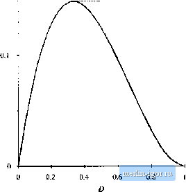
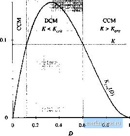
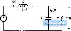
Строительный блокнот Introduction to electronics Fig. 5,12 BoosteoHvertercxanipki.  ; > dfi. tor CCM S<Aii forUCM (5,30) which is identical to the results for the buck converter. Sub.stitution of the CCM solutions for I and Д , Eqs. (2-39) and (2-43), yields (5.31) This equation can be rearranged to obtain >DD- for CCM (5.32) which is in the standard form Л>А- ;0) for CCM К<К ф) forUCM (5,33) 0,15 Fig. 5.13 Boost coiwciter X ;,(D) vs. D. 0.05  5J Boost Convener Exawpk 119 0.15 Fig. 5.14 Comparisoii i)f ATwith (0).  0.05 where K-2L The eonditions for operation in t:he eontinuous or dtseontimious eonduetion modes iire of siinilar form to those for the buck converter; however, the critical value K.-,(D) is a different function of the duly cycle D. The dependence of KjiD) on the duty cycle D is plotted in Fig. 5.13. K,.(D)h zero at D = 0 and at D= 1, and has a maxiinum value of 4/27 at D - IB. Hence, \fK is greater than 4/27, then the converter operates in the continuous conduction mode for all D. Figure 5.14 illustrates what happens when Ais less than 4/27. The converter then operates in the discontinuous conduction inode for some intennediate range of values of D near D = 1/3. But the conveiter operates in the continuous conduction mode near D = 0 and D~ I. Unlike the buck converter, the boost converterinust operate in the continuous conduction mode neiirD = 0 because the ripple magnitude approaches zero while the dc coinponent /does not. Next, let us analyze the conversion ratio M = V/V of the boost converter. When the transistor conducts, for the subinterval Q < t < D.T, the conveiter circuit reduces to the circuit of 5.15(a). The inductor voltage and capacitor current are given by (5.34) Use ofthe linear ripple approximation, to ignore the output capacitor voltage ripple, leads to .()=.- During the second subinterval DJ < t < (Di + 02)7 the diode conducts. The circuit then reduces to (5.35) Fig. S.IS Boost convener circuit;;; (a) during subinterval 1, 0 <: r < D, (b) during subinlervul 2. DT < ( < (D, + i i)7j, (c) during subinterval X i(0 L + v(() - Fig. 5.15(b). The inductor voitage and capacitor current are given by Neglect of the output capacitor voltage ripple yields v,it) = Vs-V i,f) = r(r)-  С Ф R v(,) (5.36) (.5.37) The inductor current ripple has not been neglected. During the third subinterval, (D, + 0)7, <t <T, both transistor and diode are in the off state, and Fig. 5.[5(c) is obtained. The network equations are: vl = 0, ( = 0 (5.3ю Use of the small-ripple approximation yields |