
|
| |
|
Строительный блокнот Introduction to electronics 5 J Boost Converter Example Fig. 5.1Й Inductor voltage waveform v,(r), boost converter operaiing in discontinuous conduction mode. .c = - [5.Щ Equations (5.35), (5.37), and (5.39) arc now used to sketch the inductor voltage waveform as in Fig. 5.16. By volt-second balance, this waveform must have zero dc component when the converter operates in steady state. By equating the average value of this ij(f) waveform to zero, one obtains Solution for the output voltage Vyields (5.40) (5,41) The diode duty cycle is again an unknown, and so a second equation is needed for elimination of before the output voltage V can be found. We can again use capacitor charge balance to obtain the second equation. The connection of the output capacitor to its adjacent components is detailed in Fig. 5.17. Unlike the buck converter, the diode in the boost converter is connected to the output ntxie. The mxle equation of Fig. 5.17 is (5,42) where iify is the diode cutrent. By capacitor chaige balance, the capacitor current iO) must have zero dc component in steady state. Therefore, the diode current dc component {г) tnust be equal to the dc component of the load current: So we need to sketch the diode current waveforin, and find its dc coinponent. (5.43) Fig, 5.17 Connection of the output capacitor to adjacent components In the boost converter. ;f R 4 v(f) Fig. 5.1 S Boiisl converter wiivefurms in tijc discontinuous cimductior mnde: (a) inductor current i(r), (b) diode current WO- 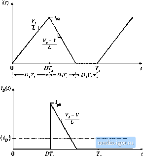 The waveforms of the inductor current til) and diode current are illustrated in Fig. 5.IS. The inductor current begins at zero, and iise.4 to a peak value ip). during the first subinterval. This peak value ij is equal to the slope V/ij, multiplied by the length of the first subinterval,/>Г,: T (5.44) The diode conducts during the second subinterval, and the inductor current then decreases to zero, where it reiuains during the third subinterval. The diode current in(f) is identical to the inductor current /(r) during the second subinterval. During the first and third subintervals, the diode is reverse-biased and hence Гд(г) is zero. The dc component of the diode current, (f), is: (5.45) The integral is the area under the ((0 waveform. As illustrated in Fig. 5.18(b), this area is the area of the triangle having peak value i, and base diinension Ол- jidt)it = iD{r, (5.46) Substitution of Eqs. (5.44) and (5.46) into Eq. (5.45) leads to the following expres.sion for the dc coinpo-nent of the diode current: 5.3 Воо.и Coinnrmr Example By equating this expression to the de load eiiirent as in Eq. (5.43), one obtains the final result (5.47) (5.48) So ntjw we have two unknowns, V atid Dj. We have two equations: Eq. (5.41) obtained via induetor volt-seeond balanee. and Eq. (5,4S) obtained using eapacitor charge balance. Let us now eliminate from this system of equations, and solve for the output voltage V. Solution of Eq. (5.41) for yields (5.49) By inserting this result into Eq. (5.48), and rearranging terms, one obtains the following quadratic equation: Use of the quadratic formula yields (5,50) (5.51) The quadratic equation has two roots: one of the roots of Eq. (5.51) is positive, while the other is negative. We already know that the output voltage of the boost converter should be positive, and indeed, from Eq. (5.41), it can be .seen that V/V must be positive since the duty cycles Bj and are positive. So we should select the positive root: (5,52) where К = 2/./ Г, valid for !<<k, {d) This is the solution of the boost converter operating in the discontinuous conduction mode. The complete boost converter characteristics, including both continuous and discontinuous conduction modes, are 1+V 1 + forA:>A (5,53) |
||||||||||||