
|
| |
|
Строительный блокнот Introduction to electronics and the dimensionless; paraitieler К = 2uri\. (b) Whtil happens lo yoLir answer Lo Part (a) for D < 0.5? (c) Derive an expression for the dt conversion ratio M{D, K). Sketch M vs. D for К = 10 anJ for Л = 0.1, over the range 0 < D < 1. DCM mode boundary analysis of die Йик converter of Fig. 5.23. The capacitor voltage ripples are small. о ЧБ ТЛПР Fig, 5,23 Cuk conveiter, Problems 5.5, 5,6, 5.11, and 5,12 R < V (a) Sketch the diode current waveform lor CCM operation. Find its peak value, in terms of the ripple magnitudes uijj, Aij; and the dc components /land/.of the two inductor currents Cf) and iV,(f), respectively. (b) Derive an expression for the conditions tinder which the Ulk converter operates in the discontin-nuns condticlion mode. Express your result in the form к < k{d\ and give formulas for kiwi К {Щ. 5.6 DCM conversion rado analysis of the Cuk converter of Fig, 5.23. (a) Suppose that the converter operates at the boundary between CCM and DCM, with the following element and parameier values: /J = 0,4 /,= 100 kHz =120У R=lQa = 54 ftH f.2 = 27 fiR C, = 47 /iF = 100 ftF Sketch the diode current waveform ijj(J), and the inductor current waveforms i{(} and i{t). Label the magnitudes ofthe ripples and dc components of these waveforms. (b) Suppose next thai the converter operates in the discontinuOu.s conduction mode, with a difierenl choice of parameter and element values. Derive an analytical expression for the dc conversion ratio M(D, K). (fi) Sketch die diode current waveform Гр((), and the inductor current waveforms f(() and i((): lor operation in the discontinuous conduction 1шч1е. 5.7 DCM nuide boundary analysis ofthe SEPIC of Fig. 5.24 (a) Sketch the diode current waveform for CCM operation. Find its peak valtie, in term,s ofthe ripple magnitudes Д£, Ai2> and the dc components / and /.he two inductor currents iO) and iiJf), respectively, (b) Derive an expression for the conditions under which the SEPIC operates in the discontinuous condticlion mode. Express your result in ihe form К v. К -((P), and give formulas for Л and 5.8 DCM conversion ratio analysis ofthe SEPIC of Fig, 5,24, (a) Suppose that ihe converter operates at the boundary between CCM and DCM, with llie follow- ПППГ Fig. 5.24 SEPIC, Problems 5.7 and 5.8. ing element and parameter value.?: D = 0.225 ICWkll?. R=iaQ V= 120V L, = 50 pH = 75 uH C=47pP С2 = 20()цГ Sketch the diode correm waveform i)(Op and the inductor current waveforms ([(() and i-it) Label the magnhudes of the ripples and dc components of these waveforms. (b) Suppose next that the converter operates in the discontinuous conduction mode, with a different choice of parameter and element values. Derive an analytical expression for the dc conversion ratio M{D, K). (c) Sketch the diode current waveform J/O. d tlie inductor current waveforms i[(f) and 12(1), for operation in the discontinuous conduction mode. An L-C input fiher is added to a btick converter as illustrated in Fig. 5.25. Inductors L and Lj and capacitor Cj are large in value, .sucli that their switching ripples are small. All losse.s can be neglected. 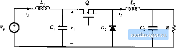 Ftg, S.2S Buck converter with input filter, Problems 5.9 atid 5.10, (a) Sketch the capacitor voltage waveform and derive expressions for its dc component K, and peak ripple magnitude Дс,. (ll) Tbe load current is increased (R is decreased in value) such that Avj is greater than V. (j) Sketch the capacitor voltage waveform Vf(t). (ii) For each subinterval, determine which semiconductor devices conduct. (ill) Determine the conditions under which the discontinuous conduction mode occurs. Express ynnr result in the form К < RrJP), and give formulas for К and A.,(,(D). 5Л0 Derive an expression for the conversion ratio M{D, K) of the DCM converter described in the previous problem. Note: D is the transistor duty cycle. 5.11 In the Cuk converter of Fig. 5.23, inductors and and capacitor Cj are large in value, such that their switching ripples are small. All losses can be neglected. (a) Assuming tliat tlie convener operates in CCM, sketch the capacitor voltage waveform Vf.(t), and derive expressions for its dc component V, and peak ripple magnitude Д1-- (b) The load current is increased {R is decreased in value) such that Av(. is greater than I,. (I) Stetch the capacitor vohage waveform v.](:). (il) For each subinierval, determine which semiconduclor devices conduct, (iii) Determine ihe conditions under which ihe discontinuous conduction mode occurs. Express your result in the form/f K(D),und give formulas for К and faJP). 5.12 Derive an expression for the conversion rado M{D, K) ofthe DCM Cuk converter described in the previous problem. Note; D is the transistor duty cycle. 5.13 A DCM btick-boost converter as in Ftg. 5.21 is to be designed to operate under the following conditions: 136V<V<204V V = - I5UV X= mm,. You may assume thai a feedback loop will vary lo transistor duty cycle as necessary to maintain a constant output voltage of - 150 V. Design the converter, subject to the following considerations: The converter should operate in the discontinuous conduction mode at all times Given the above requirements, choose the element values to minimize the peak inductor current The output voltage peak ripple should be less than IV. Specify: (a) The inductor value L (b) The output capacitor value С (c) The worst-case peak inductor current 1 (d) The maximum and minimum values ofthe transistor duty cycle D 5.14 A DCM boost converter as in Fig. 5.12 is to be designed to operate under tlie following conditions: IE V < КЗб V 3 W < f < 100 W l = 48V ./;,= 150 kHz You may assume thai a feedback loop will vary to transistor duty cycle as necessary to maintain a constant output voltage afAH V. Design the converter, subject to ihe following considerations: The converter should operate in the discondnuous conduction mode at all times. To ensure an adequate design margin, the inductance L should be chosen such that К is no greater than 15% of /f., at all operating points. Given the above requiremenis, choose the elemeni values lo minimize ihe peak inductor current. The output voltage peak ripple should be less than IV. Specify: (a) The inductor value L (b) The output capacitor value С (c) The worst-case peak inductor current r,;. |