
|
| |
|
Строительный блокнот Introduction to electronics The Ducontinuous Conduction Mode (d) The niiiKiniQiii and minimum values of die iransistorduty cycle D. (e) The values of D. К and at tlie following operating points: (i) = 1Я V and fj, = 5 W; (li) V = 36 V andP, = .5W; iii) = 18 V and P , 100 W; (i v) = 3ft V aiidP; ,= 1(Ю W. In dc-dc conveners used in battery-powered portable equipment, it is sometimes required that the converter continue to regulate its load voltage with high efficiency while the load is in a low-power sleep mode. The power required by die transistor gate drive circuitry, as well as much of the switching loss, is dependent on the switching frequency but not on lhe load currenl. So to obtain high efficiency al very low load powers, a variable-frequency control scheme is used, in which the switching frequency is reduced in proportion to the load ctirrent. Consider the boost converter system of Fig. 5.26(a). The baiiery pack consists of two nickel-cadmium cells, which produce a voltage of - 2.4 V ± 0,4 V. The converter boosts this voltage to a regulated 5 V. As illustrated in Fig. 5.26(b), the converter operates in the discontinuous conduction mode, wilh constant transistoron-dine f. The Iransistoroff-tirae 1 is varied by the controller lo regulate the otiiptii voltage. ПППГ Fig, 5.26 Boost converter employed in portable battery-powered equipment with sloop raude, Problem 5.15: (a) converter circuit, (b) inductor current wave-foiin. Baiiery pack Effective toad 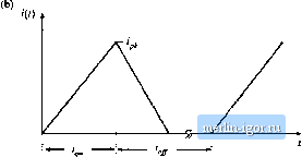 (a) Write the equations for the CCM-DCM boundary and conversion ratio M = g- in tenns of r , 1, L. and the effective load resistance Л. For parts (b) and (c), the load current can vary between ](}0pA and 1 A. The transistoron time is fixed: I MS. (b) Select values for L and С such that: * The output voUage peak ripple is no greater than 5U mV. * The converter always operates in DCM, and * The peak inductor current is as small as possible. (t) For your design of part (Ы, what are the masimtini and minimum values of the switching frequency? Converter Circuits We have already analyzed the operation of a ntimber of different types of converters: buck, btwst, buek-btrast, Ctik, voltage-sotirce inverter, etc. With these converters, a ntitnberof different ftinctions can be performed: step-dov/n of voltage, step-up, inversion of polarity, and conversion of dc to ac or vice-versa. It is natural to ask. Where do these converters come from? What other converters occur, and what other functions can be obtained? What are the basic relations between converters? In this chapter, several different circuit manipulations are explored, which explain the origins ofthe basic converters. Inversion of source and load transforms the buck converter into the boost converter. Cascade connection of converters, and simplification ofthe resulting circuit, shows how the buck-boost and Cuk converters are based on the buck and the boost converters. Differential connection ofthe load between the outputs of two or tnore convetters leads to a single-phase or polyphase inverter. A .short list of sotne of the better known convertercircuits follows this discussion. Transformer-isolated dc~4lc converters are also covered in this chapter. Use of a transformer allows isolation and multiple outputs to be obtained in a dc-dc converter, and can lead to better converter optimization when a very large or very stnall conversion ratio is required. The transformer is tnodeled as a magnetizing inductance in parallel with an ideal transformer; this allows the analysis techniqties ofthe previous chapters to be extended to cover converters containing transformers. A number of well-known isolated converters, based on the buck, boost, buck-boost, single-ended primary inductance converter (SEPIC), and Cuk, are listed and discussed. Finally, the evaluation, selection, and design of converters to meet given requirements are considered. Important perfortnance-related attributes of transformer-isolated converters include: whetherthe transformer reset process imposes excessive voltage stress on the transistors, whether the converter can supply a high-current output without imposing excessive current stresses on the secondary-side components, and whether the converter can be well-optimized to operate with a wide range of operating points, Fis- 6.1 The b.isic buck converter. ТПЛГ that is, with large tolerances in and Р,. Switch utilization is a simplified figtire-of-nierit that measures the ratio of the converter output power to the total transistor voltage and current stress. As the switch utilization increases, the converter efficiency increases while its cost decreases. Isolated converters with large variations in operating point tend to utilize their power devices more poorly than nonisolated converters which function at a single operating point. Computer spreadsheets are a gotxl tool for optimization of power stage designs and for trade studies to select a converter topology for a given application. CIRCLIT MANIPULATIONS The buck converter (Fig. 6.1) was developed in Chapter 1 using basic principles. The switch reduces the voltage dc component, and the low-pass filter removes the switching harmonics. In the continuous conduction mode, the buck converter has a conversion ratio of M = D. The buck converter is the simplest and most basic circuit, frotn which we will derive other converters. 6.1.1 Inversion of Source and Load Let us consider first what happens when we interchange the power input and pt)wer output ports of a converter. In the buck converter of Fig, 6.2(a), voltage V is applied at port 1, and voltage Vj appears at port 2. We know that k,ov, (6-1) This equation can be derived using the principle of inductor volt-second balance, with the assumption that the converter operates in the continuous conduction mode. Provided that the switch is realized such that this assutnption holds, then Eq. (6.1) is true regardless of the direction of power flow. So let us interchange the power source and load, as in Fig. fi.2(b). The load, bypassed by the capacitor, is connected to converter port 1, while the power source is connected to converter port 2. Power now flows in the opposite direction throtigh the converter. Equation (6.1) tnust still hold; by solving for the load voltage V, one obtains (6.2) So the load voltage is greater than the source voltage. Figure 6.2(b) is a boost converter, drawn backwards. Equation fi.2 nearly coincides with the familiar boost converter result, vW(D) = ШУ, except that D is replaced by D. Since power flows in the opposite direction, the standard buck converter unidirectional switch |