
|
| |
|
Строительный блокнот Introduction to electronics Port 2 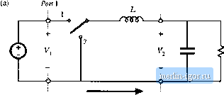 Power /low Port 1 Port 2 Fig. 6.2 Inversiun of source iind load transturms a buck converter into a boost convener: (a) buck conveiter, (b) inversion of source and loud, (c) realizaiioti of switch.  O-о a Power flow Ponl Pnrt2 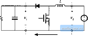 Power flow realization cannot be tised with the circuit of Fig. 6.2(h). By following the discussion of Chapter 4, one finds that the switch can be realized by eonneeting a transistor between the inductor and ground, and a diode from the inductor to the load, as shown in Fig. 6.2(c). In consequence, the transistor duty cycle D becomes the fraction of time which the single-pole double-throw (SPDT) switch of Fig. й.2(Ь) spends in position 2, rather than in position 1. So we should interchange D with its complement in Bq, ((i,2), and the conversion ratio of the converter of Fig. 6.2(c) is (6.3) Thus, the boost converter can be viewed as a buck converter having the source and load connections exchanged, and in which the switch is realized in a manner that allows reversal of the direction of power flow. Converter 1 Converter 2 Iig. 6.3 Cascade connection ufcoiwerteis. 6.1.2 Cascade Connection of Converters Converters can also be connected in cascade, as illustrated in Fig. 6.3 [1,2]. Converter 1 has conversion ratio Af ,(D), such that its output voltage Vj is (6.4} This voltage is applied to the input of the second converter. Let us assume that converter 2 is driven with the same duty cycle D applied to converter 1. If converter 2 has conversion ratio iWj(C*), then the output voltage Vis (6,S} Substitution of Et]. (6.4) into Eq. (6.5) yields (Й.6) Hence, the conversion ratio M{D) of the composite converter is the product of the individual conversion ratios M,{D) and ЩО). Let us consider the case where converter 1 is a buck converter, and converter 2 is a boost converter. The resulting circuit is illustrated in Fig. 6.4. The buck converter has conversion ratio (6.7) The boost converter has conversion ratio V - L V, ~ 1-D (6.Я) So the composite conversion ratio is 6.1 Circuit Manipulations 135 -ППЛГ Buck converter Boost converter Vi. 6.4 CaKtade comieotion o[ buck converter and boost converter.  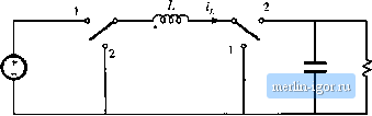 Flg, 6.S Simplification of the cascaded buck and booy converter circuit of Kig, 6.4; (a) i-einoval of capacitor Cy (b) combining of indtictorsLi and U. V D V, I-D The composite converter has a noninverting huck-hoost conversion ratit). The voltage is reduced when D < 0.5, and increased when D > 0.5. The circuit of Fig. 6.4 can he sitnpllfted considerahly. Note that inductors f ;md l, along with capacitor Cp form a Ihree-pole low-pass filter. The conversion ratio does not depend on the number of poles present in the low-pass filter, and so the same steady-state output voltage should be obtained when a simpler low-pass filter is used. In Fig. 6.5(a), capacitor C[ is removed. Inductors i.[ and L2 are ntnv in series, and can be combined into a single inductor as shown in Fig. 6.5(b). This converter, the noninverting buck-boost converter, continues to exhibit the conversion ratio given in Eq. (6.9). The switches ofthe converter of Fig. 6.5(b) can also be simplified, leading to a negative output voltage. When the switches are in position 1, the converter reduces to Fig. 6.6(a). The inductor is connected to the input source V and energy is transferred from the source to the inductor. When the |