
|
| |
Строительный блокнот Introduction to electronics 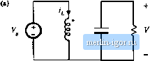 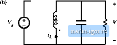 Via. 6.6 Connections of the circuit of Kig, 6.5(h}: (ii) while the iwitchcn are id position i, (h) while the swiictie are in position 2. Figi 6.7 Rcvursiii of the output voltage polarity, by reversing the intliictof coiiduciIoiik while the switches are in position 2: (a) CDiiiieciions with the switches in >osiiion !, (b) comectioiis with the switches in position 2, switches aie in position 2, the converter reduces to Fig. 6.6(b). The inductor is then connected to the load, and energy is transferred from the indtictor to the load. To obtain a negative output, we can simply reverse the polarity of the inductor during one of the subintervals (say, while the switches are in position 2). The individual circuits of Fig. 6.7 iue then obtained, and the conversion ratio becomes У D (6.10) Note that one side of the inductor is now always connected to ground, while the other side is switched between the input source and the load. Hence only one SPDT switch is needed, and the converter circuit of Fig, 6.8 is obtained. Figure 6.8 is recognized a.s the conventional buck-boost converter. Thus, the buck-boost converter can be viewed as a cascade connection of buck and boost converters. The properties of the buck-boost converter are consistent with this viewpoint. Indeed, the equivalent circuit model of the btick-boost converter contains a 1:D (buck) dc transformer, followed by a РЛ (boost) dc transformer. The buck-boost converter inherits the pulsating input current of the buck converter, and the pulsating output current of the boost converter. Other converters can be derived by cascade connections. The cuk converter Fig. 2.20) was originally derived [1,2] by cascading a boost converter (converter 1), followed by a buck (converter 2). A negative output voltage is obtained by reversing the polarity of the internal capacitor connection during one of the subintervals; as in the buck-boost converter, this operation has the additional benefit of reducing the nuntber of switches. The equivalent circuit model of the Cuk converter contains a 1У\ I (boost) Fly. Ct)nve] ter eiictiit obtaitied Га>т the . subcircuitsof Fig. 6,7. f+J 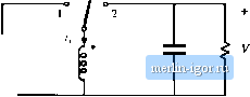 ideal de transformer, followed by a 1:D (biiek) ideal dc transformer. The converter inherits the non-pulsating input current property of the boost converter, and the nonpulsating output current property of the buck converter. 6.1 J Rotation of Three-Terminal Cell The buck, boost, and buck-boost converters each contain an inductor that is connected to a STOT switch. As illustrated in Fig. 6.9(a), the indue tor-switch network can be viewed as a basic cell having the three terminals labeled Л, h, and c. It was first pointed out in [1,2], and later in [3], that there are three distinct ways to connect this cell between the source and load. The connections a-A h-B c~C lead to the buck converter. The connections a-C b-A c-B atnount to inversion of the source and load, and lead to the boost converter. The connections a~A b-C c~B lead to the buck-boost converter. So the buck, boost, and buck-boost converters could be viewed as being based on the same inductor-switch cell, with different source and load contiections. Adual three-terminal network, consisting of a capacitor-switch cell, is illustrated in Fig.6.9(b). Filter inductors are connected in series with the source and load, such that the converter input and output currents are nonpulsating. There are again three possible ways to connect this cell between the source and load. The connections я-Л h~B c~C lead to a buck converter with L-C input low-pass filter. The connections a-B b-A c-C coincide with inversion of source and load, and lead to a boost converter with an added output L-C filter section. The connections a-A b~Cc~B lead to the Cuk converter. Rotation of more ctmiphcated three-terminal cells is explored in [4]. 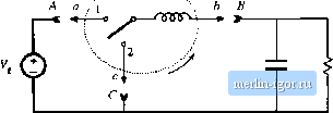 ТППГ A ai \± hi \ b в тллг ... с ЧС Fig. 6.9 Rotation of three-terminal switch cells: (a) switch/inductor cell, (b) switchycapacltor cell. dc source load © Converter 1 ~T 1 Converter 2 Vig, 6.10 Obtaining ii bipolar output by diHtirential connection of load. 6.1A DifTerentJal Connection of the Load In iuverter applications, where an ac output i.s required, a converter is needed tliat is capabie of producing an output voltage of either polarity. By variation of the duty cycle in the cotrect manner, a .sinusoidal output voltage having no dc bias can then be obtained. Of the converters studied so far in this chapter, the buck and the boost can produce only a positive unipolar output voltage, while the btick-boost and Cuk converter produce only a negative unipolar output voltage. How can we derive converters that can produce bipolar output voltages? A well-known technique for obtaining a bipolar output is the differential connection of the load across the outputs of two known converters, as iihi.strated in Fig. 6.10. If converter 1 produces voltage Vp and converter 2 produces voltage Vj, then the load voltage Vis given by K= V,-V, (6.11) Although V[ and mayboth individually be positive, the load voltage Vcan be cither positive or itega-tive. Typically, if converter 1 is driven with duty cycle Д then converter 2 is driven with its complement, O, so that when increases, Vj decrea.4es, and vice versa. Several well-known inverter circuits can be derived using the differential connection. Lets realize converters ! and 2 of Fig. fi.lO using buck converters. Figure 6.11 (a) is obtained. Converter 1 is driven with duty cycle Д while converter 2 i.s driven with duty cycle P. So when the SPDT .switch of converter 1 is in the upper position, then the SPDT switch of converter 2 is in the lower position, and vice-versa. Converter 1 then produces output voltage V, = DV, while converter 2 produces output volt- |