
|
| |
|
Строительный блокнот Introduction to electronics Principles of Steady-State Converter Analysis INTBODUCTION In the previous chapter, the buck converter was introduced as a means of reducing the dc voltage, using only nondissipative switches, inductors, and capacitors. The switch produces a rectangular waveform v,(f) as illustrated in Fig. 2.1. The vohage v,(0 is equal to the dc input voltage V when the switch is in position 1, and is equal to zero when the switch is in position 2. In practice, the switch is realized using  Switch position: Fig, 2.1 Heal switch, (n), used to reduce the voltage dc component, and (b) its output voltage waveform v(i). Fig. 2.2 Delemiination of (he switch output voltage dc ccmpiinent, by iniegralitig and dividing by the switching period.
power semiconductor devices, such as transistors and diodes, which are controlled to turn on and off as required to perform the function of the ideal switch. The switching frequency equal to the inverse of the switching period generally lies in the range of 1 kHz to 1 MHz, depending on the switching speed of the semiconductor devices. The duty ratio D is the fraction of time that the switch spends in position 1, and is a number between zero and one. The complement of the duty ratio, D, is defined as (1 ~ D). The switch reduces the dc component of the voltage: the switch output voltage v/() has a dc component that is less than the converter dc input voltage V. From Fourier analysis, we know that the dc component of v,(0 is given by its average value v,), or <2.1) As illustrated in Fig. 2.2, the integral is given by the area under the curve, or DTV. The average value is therefore (2.2) So the average value, or dc component, of v{t) is equal to the duty cycle times the dc input voltage V. The switch reduces the dc voltage by a factor of D. What remains is to insert a low-pass filter as shown in Fig. 2.3. The filter is designed to pass the dc component of v,{f), but to reject the components of v,(t) at the switching frequency and its harmonics. The output voltage v(r) is then essentially equal to the dc component of v,(r)r (2,3) The converter of Fig. 2.3 has been realized using k)ssless elements. To the extent that they are ideal, the inductor, capacitor, and switch do not dissipate power For example, when the switch is closed, its voltage drop is zero, and the current is zero when the switch is open. In either case, the power dissipated by the switch is zero. Hence, efficiencies approaching 1Ю% can be obtained. So to the extent that the components are ideal, we can realize our objective of changing dc voltage levels using a lossless network. 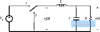 Fit;. 2,3 Inaeriion of low-pass (liter, to lemove the switching liarmonitfi and pass only tJ>e lic componcni of vj,t) tu tlie output. 2.2 Inductor Volt-Second Balance, Capacitor Charge Balance, and the Small-Ripple Approximauon 15 Fig. 2A Buck converter etc output vollage V vs. duty cycle D. The network of Fig. 2.3 also allows control of the output, Figure 2,4 is the control characteristic of the converter. The output voltage, given by Eq. (2.3), is plotted vs. duty cycle. The buck converter has a linear control characteristic. Also, the output voltage is less than or equal to the input voltage, since 0<f>< (.Feedback systems are often constructed that adjust the duty cycle D to regulate the converter output voltage. Inverters or power amplifiers can also be built, in which the duty cycle varies slowly with time and the output voltage follows. The buck converter is just one t)f many possible switching converters. Two other commonly used converters, which perform different voltage conversion functions, are illustrated in Fig. 2.5. In the boost converter, the positions of the inductor and switch are reversed. It is shown later in this chapter that the boost converter steps the voltage up: Vk Vj,. Another converter, the buck-boost ctmverter, can either increase or decrease the magnitude of the vtdtage, but the polarity is inverted. So with a pt)sitive input voltage, the ideal buck-boost converterciin produce a negative output voltage of any magnitude. It may at first be surprising that dc output voltages can be produced that are greater in magnitude than the input, or that have opposite polarity. But it is indeed possible to produce any desired dc output voltage using a passive network of only inductors, capacitors, and embedded switches. In the abtne discussion, it was possible to derive an expression for the output vt)ltage of the buck ctmverler, Eq, (2.3), using some simple arguments based on Fourier analysis. However, it may not be immediately obvious how to directly apply these arguments to find the dc output voltage of the boost, buck-boost, or other converters. The objective of this chapter is the development of a more general method for analyzing any switching converter comprised of a network of inductors, capacitors, and switches [1-8]. The principles of inductor volt-secot\d balance and capacitor charge balance are derived; these can be used to solve for the inductor currents and capacitor voltages of switching converters. A useful approximation, the small-ripple or linear-ripple approximation, greatly facilitates the analysis. Some simple methods for selecting die filter element values ate also discussed. 2.2 INDLtTOR VOLT-SECOND BALANCE, CAPACITOR CHARCE BALANCE, AND THE SMALL-RiPPLE APPROXIMATION Let us more closely examine the inductor and capacitor waveforms in the buck converter of Fig. 2,6, It is impossible to build a perfect low-pass filter that allows the dc component to pass but completely removes the components at the switching frequency and its harmonics. So the low-pass filter must allow at least some small amount of the high-frequency harmonics generated by the switch to reach the output. Hence, in practice the output voltage waveform v{t) appears as illustrated in Fig. 2.7, and can be expressed as So the actual output voltage v(/) consists of the desired dc component V, plus a small undesired ac com- |
|||||||||