
|
| |
|
Строительный блокнот Introduction to electronics Fig. 6,38 Wavufomis of thu isolated SEPIC, condiiuous condutiioii mode. kit) Conducting devices: DT, {iy--iiln \ netizing inductance performs the energy-storage function of the original inductor l. In addition, the ideal transformer provides isolation and a turns ratio. Typical primary and secondary winding current waveforms iif) and are portrayed in Fig 6.38, for the continuous conduction mode. The magnetic device must function as both a flyback trans former and also a conventional two-winding transformer. During subinterval 1, while transistor Qj con ducts, the magnetizing current Hows through the primary winding, and the secondary winding current is zero. During subinterval 2, while diode Dj conducts, the magnetizing current flows through the second ary winding to the load, In addition, the input inductor current i,ilows through the primary winding. This induces ati additiotial component of .secondaty curretit ifti, which also flows to the load. So design ofthe SEPIC transformer is somewhat unusual, and the rms winding currents are larger than those ofthe flyback transformer. By application ofthe principle of volt-second balance to inductors L and L, the conversion ratio can be shown to be Ideally, the transistor must block voltaiie VJD. In practice, additional voltage is observed due to ringing associated with the transformer leakaiie inductance. Comener Circuits 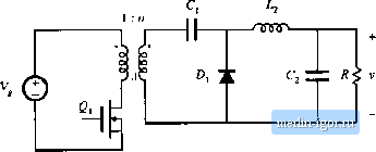 Пй. 6.3!) Isolated iiiveise-SEPIC, All isolated version of the inverse-SEPiC is shown in Fig. fy?9. Operation and design of the transformer i.s similar to that of the SEPIC. Isolation in the Cuk converter is obtained in a different manner [181. The basic nonisolated Cuk converter is illustrated in Fig. 6.4()(a). In Fig. 6.40(b), capacitor C is split into two series capacitors C[ and C[j,. A transforiner can now be inserted between these capacitors, as indicated in Fig. 6.40(c). The polarity marks have been reversed, so that a positive output voltage is obtained. Having capacitors in series with the transformer primary and secondary windings ensures that node voltage is applied to the transforiner. The transforiner functions in a conventional manner, with small inagnetizing current and negligible energy storage within the magnetizing inductance. Utilization of the transformer of the Uuk converter is quite good. The magnetizing current can Pig, 6,40 Obtaining isolation in the Cuk convener: (a) basic nonisolatetl Cvk converter, (b) splitting capacitor C into two scries capacitors, (c) insertion of traii.sformcf between capacitors. 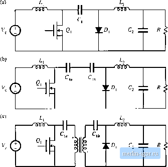 ! :n 6.4 Convener Evaluatiofi and Denign 171 be both positive and negative, and hence the entire tore B-H loop can be utilized itdesired. There are no center-tapped windings, aud all ofthe copper is effectively utilized. The tran.sistor must block voltage V/Dp plus some additional voltage due to ringing associated with the transformer leakage inductance. The conversion ratio is identical to that of the isolated SEPIC, Eq. (6.50). The isolated SEPIC and duk converter find application as switching power supplies, typically at power levels of several hundred watts. They are also now finding use as ac~dc low-harmonic rectifiers. 6.4 CONVERTER EVALUATION AND DESIGN There is no ultimate converter perfectly suited for all possible applications. For a given application, with given specifications, trade studies should be performed to select a converter topology. Several approaches that meet the specifications should be considered, and for each approach important quantities such as worst-case transistor voltage, worst-case transistor rms current, transformer size, etc., should be computed. This type of quantitative comparison can lead to selection of the best approach, while avoiding the personal biases of the engineer. 6.4.1 Switch Stress Utilizatiun Often, the largest single cost in a converter is the cost of the active semiconductor devices. Also, the conduction and switching losses associated with the semiconductor devices often dominates the other converter k)sses. This stiggests evaluating candidate converter approaches by comparing the voltage and current stresses imposed on the active semiconductor devices. Minimization of the total switch stresses leads to miniinization ofthe total silicon area required to realize the power devices of the converter. So it is useful to compare the total active switch stress and active switcli utilization of candidate converter approaches. In a good design, the voltages and currents imposed on the semiconductor devices is minimized, while the k)ad power is maximized. If a converter contains i: active semiconductor devices, the total active switch stress S can be defined as (6,51) where Vj is the peak voltage applied to semiconductor switch j. and Ij is the rms current applied to switch / Peak rather than rms current is sometimes used, with qualitatively similar results. If the converter load power is Pi j, then the active switch utilization U can be defined as /1 - (6,52) The switch utilization is less than one in transformer-isolated converters, and is a quantity to be maximized. For example, consider the transistor utilization in the CCM flyback converter of Fig. 6.30(d). The peak transistor voltage occurs during subinterval 2, and is equal to the dc input voltage plus the reflected load voltage VAr |