
|
| |
|
Строительный блокнот Introduction to electronics [6] F. Earzegar and S.Cuk , A New Switthed-Mode Amplifier Produces Clean TKree-Piiase Power, Pro- ceedings Ninth IwermitionalSolid-State Power Conversion Conference (Powercon 9), pp. E3.!-E3.!5, Juiy 1982. (7] K. D. T. Kgo, S. Cuk, and R. D. MlDDLEBROOK, A New Flybiick Dc-[i)-Three-Pli.ise Convener wilh Sinusoidal Outputs, IEEE Power Electronics Specialists Conference. 19S3 Record, pp. 377-388. [S] R. W. Ericksok, Synthesis of Switched-.VIode Converters, IEEE Power Electronics Specitilists Confer- ence, 1983 Record, pp. 9-22, June 5983. [9] D. Mak.SiMOVIC and S. Cltk, General Properties and Synthesis of PWM Dc-Dc Converters, IEEE Power Electronics Specialists Conference, 5989 Record, pp. 515-525, June 1989. [10] M. S. .VlAKOWSKi, On Topological Assumptions on PWM Converters-A Reexamination, IEEE Power Electronics Specialists Conference, 1993 Record, pp. 145-147, June 1993. [11] E. israelsen, J. MARTIN, C. REEVE, and V. ScowN, A 2.5 kV High Reliability TWT Power Supply: Design Techniques for High Efficiency and Low Ripple, IEEE Pnwer Electronics Specialists Conference, 5 977 Record, pp. 109-130, June 1977. [12] R. Severns, A New Current-Fed Converter Topology, JEEE Power Electronics Speciali.ts Conference. 1979 Record, pp. 277-2S3, June 5979. [13] V. J. ThottuvelIL, T. G. Wilson, and H. A. Owen, Analysis and Design of a Push-Pull Current-Fed Converter, IEEE Power Electronics Specialists Conference, 1981 Retool, pp. 192-203, June 1981. [14] R. Redl AND N. sokal, Push-Pul! Current-Fed Multiple-Output Dc-Dc Power Converter wilh Only One Inductor and with 0-100% Switch Duty Ratio, IEEE Power Electronics Specialists Conference, 1980 Record, pp. 341-345, Juiie 1982. [15] p. W. Cl.vrke, Converter Regulation by Controlled Conduction Overlap, U. S. Patent 3,935,024, Febtu-шу SO, 1976, [!6] R. p. Massey and E. C. Snyder, High-Voitage Single-Ended Dc-Dc Convener, IEEE Power Electronics Specialists Cimferetice, 1977 Record, pp. 156-159, June 1977. [17] D. MakIMOVic: and S. CLK, Switching Converters with Wide DC Conversion Range, IEEE Trrtii.iac-titms on Power Electronics, Vol.6, No. i, pp. 151-157, January 1991, [IS] R. D. MlDDLEBROOK and S. CUK, Isolation and Multiple Outputs of a New Optimum Topology Switching Dc-io-Dc Converter, IEEE Power Electicmic.i Specialists Conference. 197S Record, pp. 256-264, June 13*15, 1978. [19] T. G. wilson , Cross Regulation in an Energy-Storage Dc-to-Dc Convener with Two Regulated Outputs, IEEE Power Electronic.. Speciali.its Conference, 1977 Record, pp. 19Q-199, June 1977. [20] H. Matsuo, Comparison of Multiple-OLitpui Dc-Dc Converters Using Cross Regulation, IEEE Power Electronics Speciali.its Conference. 1979 Record, pp. 169-185, June 1979. [21] k. Harada, T. Nabeshlma, and k. Hi.sanaga, State-Space Analysis of the Cross-Regulation, JEEE Power Electronics Speciali.vts Conference, 1979 Record, pp. 186-192, June 1979. [22] J. N. Park and T. R. ZALOUM, A Dual Mode ForwarjyFlybatk Convener, IEEE Power Electronic! Spe-ciiilists Conference, 1982 Record, pp. 3-13, June 19S2. [23] S. ClJK, General Topological ftoperEies of Switching Slruclures, IEEE Power Electronics Specialists Софгепсе. 1979 Record, pp. 109-130, June 1979. [24] R. SEVERNS and G. BLOOM, Modem Dc-to-Dc Swstchinode Power Converter Circuits, New York: Van NoslrandReinhold, 1985. [25] N. мон.лк, Т. UnDEL.ND, and W. ROEEINS, Pfnifr Electronics! Converters. Applications, and Design, 2 edit.. New York: John Wiley & Sons, 1995. [26] J. KASSAKIAN, M. SCHLECHT, and G. VEROHESE, Principles of Power Eleclromcs, Reading, MA: Addi-son-Wesley, 1991. [27] D. Mitchell, Dc-Dc Switchmg Regulator АпаЫ.ч, New York: McGraw-Hill, 1988. [2S] K. Kit Sum, Switch Mode Power Conversion: Basic Theory and De.sign, New York: Marcel Dekker, 1984. [29] R. E. Tarter, Solid-Stale Power Conversion Handbook, New York: John Wiley & Sons. 1993. [30] Q. CHEN, F. C. Lee. and m. M. JOVANOVtC, DC Analysis and Design of Multiple-Output Forward Converters with Weighted Voltage-Mode Comro\f IEEE Applied Power Elecrronks Conference, 1993 Record, pp. 449-455, March 1993. Problems 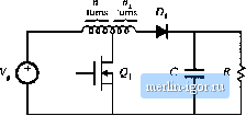 Fig. 6,41 Tapped-inductor boost converter. Problem 6.1 Tapped-in due tor boost converter. The boost converter is sumeiimes modified as illustrated in Fig. 6.41. to obtain a larger conversion ratio than would otherwise occur. The inductor winding contains a total ot (fj + lij) turns. The transistor is connected to a tap placed ii turns from the left side of the inductor, a.s shown. The tapped inductor can be viewed as a two-winding (1:Ч2) transformer, in which the two windings are connected in series. The indactimce of the entire (n, -t- i!j) turn winding is L. (a) Sketch an equivalent circuit model Ior the tapped inductor, which includes a magnetising inductance and an ideal transformer. Label the values ofthe magnetizing Inductance and turns ratio. (b) Determinean analytical expression for the conversion ratio M = VVV,. You may assume thatthe transistor, diode, tapped inductor, and capacitor are lossless. You may also assume that the converter operates in c()ntimious conduction mode. (c) Sketch M(D) vs. D for fi, = Jij, and compare to ihenontapped { j = 0) case. Analysis of ihe DCM flyback cnnverter. The flyback converter of Fig. 6.30<d) nperates in the dlscontinu-onsconductionmode. (я) Model the flyback transfomner a.s a magnetizing inductance in parallel with an ideal transformer. Eind sketch the converter circuits during itie tliree subintervals. (b) Derive the conditions for operation in di.scontiimous conduction mode. (c) Solve the converter: derive expressions for the steady-state output voltage V and subintcrvai 2 (diodeconduction interval)duty cycle Oj. AnaJysis of the isolated inverse-SEPIC of Fig. 6.39. You may assume that the converter operates in Itie continuous conduction mode, and that all inductor current ripples and capacitor voltage ripples are small. (a) Derive expressions for the dc components of ttie magnetizing current, inductor current, and capacitor voltages. (b) Derive analytical expressions for therms values of the primary and secondary winding currents. Note that these quantities do not simply scale by the turns ratio. The two-transi.stor tlyback converter. The converter of Fig. 6.42 is sometimes used when the dc input voltage is high. Transistors and Q2 are driven with the same gating signal, such that they turn on and off simultaneously with the same duty cycle D. Diodes П, and ensure that the off state voltages of the transistors do not exceed V. The convener operates in discontinuous conduction mode. The magnetizing inductance, referred to the primary side, is L- Fig. 6.42 TWo-transistor flyback couvcrtet, Problem 6,4. 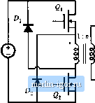 (a) Determine an analytical expression for the steady-state output voltage V. (b) Over what range of duty cycles does the transformer reset properly. Explain. A nonideal flyback cnnverter. The flyback converter shown in Fig. 6.3u<d) operates in the continuous conduction mode. The MOSFET has on-resistance R and the diode has a constant forward voltage drop Vq. The tlvhack triaisformer has primar> windine resistance Д, and secondar> winding resistance (a) Derive a complete steady-state equivalent circuit model, which is valid in the continuous conduction mode, and which correctly models lhe loss elements listed above as well as the converter input and output ports. Sketch your equivaleni circuit. (h) Derive an analytical expression for the converter efficiency. A low-volt age computer power supply with synchronous rectification. Ttie trend in digital Integra ted circuits is towards lower power supply voltages. It is difficult to construct a high-efficiency low-voltage power supply, because the conduction loss arising in lhe secondary-side diodes twcomes ver> large. The objective of this problem is 10 estimate tiow lhe efficiency of a forward converter varies as the output voltage is reduced, and to investigate the use of synchronous rectifiers. The forward converter of Fig. 6.22 operates from a dc input of = 325 V, and supplies 20 A to its dc load. Consider three cases: (i) V.= 5 V, (ii) V= 3.3 V, and (ш) V= 1.5V. For each case, the turns ratio Mj/n, is chosen such that the converter produces lhe required output voltage at a tian.si.stor duty cycle of £> = 0.4. The MOSFET has on-iesistauce = 5 Й. The .secondary-side schottky diodes have |