
|
| |
|
Строительный блокнот Introduction to electronics Problems forward voltage drops of V-0.5 V, All other elements can be considered ideal. (a) Derive an equivalent circuit for the forward converter, which models the semiconductor conduction losses described above. (b) Solve your model for cases (/), (Ii), and (Iii) described above. For each ca.se, determine numerical values ofthe turns ratio й,/*!, and for theefficiency T\. ((} The secondary-side Schottky diodes are replaced by MOSFETs operating as synchronous rectifiers. The MOSFETi each have an on-resistance of 4 ttlii. Determine the new numerical values ofthe tiims ratio n-Jn and the efficiency T), forcases (i>, (ii), and (iii). Rotation of switching cells. A network containing switches and reactive elements has terminals o, l\ and c, as illustrated in Fig. 6.43(a). You are given that the relationship between the terminal voltage.s is V,/V,-tL(iy).
1 :n Fig, 6.43 Rotation of three-terminal switching cells, ftoblem 6.7 (a) Derive expressions for the source-to-load conversion ratio V7V = M(D), in terras of li(D), for the following three connection schemes: (i) o-Ah-Bc-C (ii) a-B h-C c-A {iii) a-Ch-A c-B (b) Consider the three-terminal network of Fig. 6.43(b). Determine fl(fJ) for this network. Plug your answer into your results from part ta), to verify that the buck, boost, and bnck-boost converters are generated. (c) Consider the three-terminal network of Fig. 6.43(c). Determine ji-iD) forthis network. Plug your answer into your results from part (a). Whit converters are generated? Transformer-isolated current-sense circuit. It is often reijuired that the current flowing in a power transistor be sensed. A noninduclive resistor R placed in series with the transistor will produce a voltage v(() that is proportional to the transistor drain current Use of a transformer allows isolation between the power transistor and the control circuit. The tran.sformer turns ratio also allows reduction ofthe current and power loss and increase ofthe voltage ofthe resistor. This problem is concerned with design t>f the transformer-isolated current-sense circuit of Fig. 6.44. 1 ;и Fig. 6.44 Transformer-ibOlated circuit lra- sensing the transistor switch curretit, Problem 6.R R < vit) Ttie transforiner tias a single-turn primary and -ш. n-Lurn secondaiy winding. Ttie transistor switches on and off with duty cycle D and switching frequency While ttie transistor conducts, its current is essentially constant and is equal to /. Diodes D, and D, are conventional silicon diodes having forward voltage drop V,-,. Diode Dj, is a zener diode, which can be modeled as a voltage source of value V, witli die polarity indicated in the figure. For a proper design, the circuit elements should be chosen SQch lhat the transformer magnetizing current, in conjunction with diode Oj, operates in discontinuous conduction mode. ]□ a good design, the magnetizing current is much smaller than the transistor current. Thiee subintervals occur during each switching period; subinterval 1, in which and conduct; sub-interval Z, in which Я2 ind conduct; subinterval 3, in wliich Sj, Л, and fJj are off. (Ъ) it) (d) Sketch the current sense circuit, replacing the transformer and lener diode by their equivalent circuits. Sketch the waveforms of Ihe transistor current iff), the transforiner magnetizing current iff{(), the primary winding voltage, and the voltage v{!). Label salient features. Determine tlie conditions on the zener voltage Vj, thai ensure that the transformer magnetizing current is reset lo zero befnne the end of the switching period. You are given the following specifications: Switching frequency Transistor duly cycle Transistor peak current 1110 kHz D < 0.73 тал f,j(0 < 25 A The output voltage vff) should equal 5 V when the transistor current is 25 A, To avoid saturating the transformer core, the volt-seconds applied to tlie single-turn primary winding while the transistor conducts should be no greater than 2 volt-isec. The silicon diode foiward voltage drops are Vo = 0.7 V. Design the circuit: select values of Й, л. and V, 6.9 Optimal reset of the fonvard converter transfoimei. As illustrated in Fig. 6.45, it is possible to leset the transformer of the forward converter using a voltage source other than the dc input V; several such schemes appear in the literature. By optimally choosing the value of the reset voltage V, the peak voltage stresses imposed on transistor Ci and diode can be reduced. The maximum duty cycle can also be increased, leading 10 a lo4ver iransformer turns ratio and lower iransistor current. Tlie resulting improvement in converter cost and efficiency can be significant when the dc input voltage varies over a wide range. (a) As a function of V the transistor duty cycle D. and the transformer turns ratios, what is the minimum value of V, that causes the transformer magnetizing current to be reset to zero by Lhe end of the switching peiiod? (b) For your choice of from part (a), whai is the peak voltage imposed 011 transistorQ,? This converter is to t>e used in a universal-inpnt off-line application, with lhe following speciricatioiis. The input voltage V, can vary between 127 and 3W V. The load voltage is regulated by variation of the 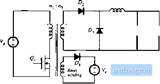 fig. 6.45 Forward converter with auxiliary reset windtttg, Problctr 6,У duty cycle, and is equal lo 12 V. The load power is 480 W. (c) Choose the turns ratio ii/u such that the total acdve switch stress is rainimi/ed. For your choice of /!j/ j,over what range will the duty cycle vary? What is the peak transistor current? (d) Cimipare your design of Part (cf with the conventional scheme in which II, - il- and - V. Compare the worst-case peak transistor voltage and peak transistor current. (e) Suggest a way lo implement the voltage source V, Give a schematic of the power-stage components of your implementation. Use a few sentences lo describe Ihe control-circuit functions required by your implementation, if any. 6.10 Design of a multiple-output dc-dc flyback converter. For this problem, you may neglect all losses and transformer leakage inductances. It is desired that the three-output flyback converter shown in Fig. 6.46 operates in the discontinuous conduction mode, with a switching frequency of f - lOOkllz. The nominal operating conditions are given in the diagram, and you may thai there are no variations in the input voltage or the load currents. Select fJ, = 0.1 (the duty cycle ot subinterval 3, in which all semiconductors are off). The objective of this problem is lo find a giiod steady-slate design, in which the semiconductor peak blocking voltages and peak currents are reasonably low. 165 Vdc 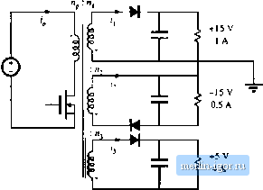 Fig, 446 Three-outpLit flyback converter design. Problem 6.10. |
|||||||||||||||