
|
| |
|
Строительный блокнот Introduction to electronics t7,3) So we will employ the basic approximation trfremoving the high-frequency switching ripple by averaging over one switching period. Yet the average value i.s allowed to vary frotn one switching period to the next, such that low-frequency variations are modeled. In effect, the moving average of Eq. (7,3) constitutes low-pass filtering of the waveform, A few of the numerous references on averaged modeling of switching converters ate listed at the end of this chapter [1-20]. Note that the principles t>f inductor volt-second balance and capacittw charge balance predict that the right-hand sides t)f Eqs. (7.2) are zero when the converter tjperates in equilibriutn. Equations (7.2) de.scribe how the inducttir current.s and capacittir vtjltages change when nonzert) average inductor voltage and capacitor current are applied over a switching period. The averaged inductor voltage and capacitor currents of Eq. (7.2) are, in general, nonlinear funttitKis of the signals in the converter, and hence Eqs. (7.2) constitute a set of nonlinear differential equatitms. Indeed, the spectrum in Fig. 7.3 also contaitis hartnonics tjf the mtrfulation frequency ti), . In most converters, the.se harmonics becotne significant in tnagnttude as the modulation frequency U) approaches the switching frequency 0), or as the modulation amplitude 2J, approaches the quiescent duty cycle D. Nonlinear elements are not uncommon in electrical engineering; indeed, all semiconductor devices exhibit nonlinear behavior. To obtain a linear model that is easier to analyze, we usually construct a small-signal model that has been linearized about a quiescent operating ptnnt, in which the harmonics t)f the mtjdulatitjti t>r excitation frequency are neglected, .As an example. Fig. 7.4 illustrates linearization of the familiar diode i~v characteristic shown in Fig. 7.4(b). Suppose that the diode current i(Ohas a quiescent (dc) value / and a signal component lit). As a result, the voltage i(/) across the diode has a quiescent value Vand a signal component v(0. If the signal components are small cotnpared to the quiescent values, then the relationship between v(0 and f(f) is approximately linear, v(/) = ГдгСО- The conductance l/r  V = V+v 3a-2a- 1 a- Acluii! nonlinear, characteristic Ab Utuurized Quiescent if futiction operatitig f 0,5 V Fig. 7.4 Stnall-signal equivalent circuit modeling nrtlicdiodi;: (a) a nonliuoar diode couductittg current i; (b) linearization of tile diode characteristic around a quiescent operating point; (c) a tiiieuriz-ed small-signal model. 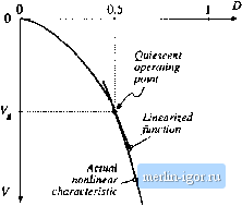 Fig. 7.5 Linearization cii tile static control-to-outptit characteristic of tlto buck-botist converter about tlie quiescent operating ptiint D - 0 1. represents the slope ofthe diode characteristic, evaluated at the quiescent operating point. The small-signal equivalent circuit model of Fig. 7.4(c) describes the diode behavior for small variations around the quiescent operating point. An example of a nonlinear ctuiverler characteristic is the dependence of the steady-state output voltage V of the buck-boost converter on the duty cycle D, illustrated in Fig, 7.5. Suppose that the converter operates with some dc output voltage, say, V - - V, conesponding to a quiescent duty cycle of D = 0.5. Duty cycle variations cl about this quiescent value will excite variations v in the output voltage. If the magnitude ofthe duty cycle variation is sufficiently small, then we can compute the resulting output voltage variations by linearizing the curve. The slope of the linearized characteristic in Fig. 7.5 is chosen to be equal to the slope ofthe actual nonlinear characteristic at the quiescent operating point; this slope is the dc control-to-output gain ofthe converter. The linearized and nonlinear characteristics are approximately equal in value provided that the duty cycle variations rf are sufficiently small. Although it illustrates the process of small-signa! linearization, the buck-boost example of Fig. 7.5 is oversimplified. The inductors and capacitors of the converter cause the gain to exhibit a frequency response. To correctly predict the poles and zert>es ofthe small-signa! transfer fimctions, we must linearize the converter averaged differential equations, Eqs, (7.2). This is done in Section 7.2. A small-signal ac equivalent circuit can then be constructed using the methods developed in Chapter 3. The resulting small-signal model of the btick-boost converter is illustrated in Fig, 7,6; this model can be solved using conventional circuit analysis techniques, to find the smalt-signal transfer functions, output impedance, and other frequency-dependent properties. In systems such as Fig. 7.1, the equivalent circuit mode! can be inserted in place of the converter. When small-signal models ofthe other system elements (such as the р,(/)ф f</(oQ 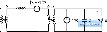 Fig, 7.Й Small-signal ac equivalent circuit mode! of tile buck-boost conveiter. pulse-width modulator) are inserted, then a complete linearized system model is obtained. This model can be analyzed using standard lineac techniques, such as the Laplace transform, to gain insight into the behavior and properties of the system. Two well-known variants of the ac modeling method, state-space averaging and circuit averaging, are explained in Sections 7.3 and 7.4. An extension of circuit averaging, known as i:i\vi-af>ed switch nwdeling, is also discussed in Section 7.4. Since the switches are the only eletnents that introduce switching harmonics, equivalent circuit models can be derived by averaging only the switch waveforms. The converter models suitable for analysis or simulation are obtained simply by replacing the switches with the averaged switch model. The averaged switch modeling technitjue can be extended to other modes of operation such as the discontinuous conduction mode, as well as to current programmed control and to restmant converters. In Section 7.5, it is shown that the small-signal mode! of any dc-dc pulse-width modulated CCM converter can be written in a standard form. Called the camitical model, this eciuivalent circuit describes the basic physical functions that any of the.se converters must perform. A simple mode! of the pulse-width modulator circuit is described in Section 7.6. These models are useless if you dont know how to apply them. So in Chapter S, the frequency response of converters is explored, in a design-oriented and detailed manner. Stnall-signa! transfer functions of the basic converters are tabulated. Bode plots of converter transfer functions and impedances are derived in a simple, approximate manner, which allows insight to be gained into the origins of the ffe-(juency response of cotnplex converter systems. These results are used to design converter control systems in Chapter 9 and input fdters in Chapter 10. The modeling techni(]ues are extended in Chapters 11 and 12 to cover the discontinuous conduction mode and the current programmed mode. THE BASIC AC MODELING APPROACH Let us derive a smalt-signal ac model of the buck-boost converter of Fig. 7.7. The analysis begins as usual, by determining the voltage and current waveforms of the inductor and capacitor When the switch is in position t, the circuit of Fig. 7.8(a) is obtained. The inductor voltage and capacitor current are: (7,5) ----r (7.6) We now make the small-ripple approximation. But rather than replacing and v(f) with their dc components and V as in Chapter 2, we now replace them with their low-frequency averaged values (*j,(f))]., and (v(())y, defined by Eq. (7.3). Equations (7.5) and (7.6) then become 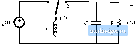 rig. 7,7 Bock-boost converter example. |