
|
| |
|
Строительный блокнот Introduction to electronics 2.2 Inductor Voli-Secoiid balance, Capaciwr Charge Balance, and the Small-Ripple Approsinuition 19 position 1, and the process repeats. h is of interest to calculate the inductor current ripple Д(. As illustrated in Fig. 2.10, the peak inductor current is equal to tlie dc component / plus the peak-to-average ripple Д/. This peak current flows through not only the inductor, hut also through the semiconductor devices that comprise the switch. Knowledge of the peak current is necessary when specifying the ratings of these devices. Since we know the slope of the inductor current during the first subinterval, and we also know the length of the fust subinterval, we can calculate the ripple magnitude. The J,(f) waveform is symmetrical about /, and hence during the first subinterval the current increases by ЗЛУ, (since Д/ is the peak ripple, the peak-to-peiik ripple is 2Ai,). So the change in current, 2Af is equal to the sk)pe (the applied inductor voltage divided by L) times the length of the first subinterval (-ОГ: (change in i,) = (slopeKlenglh of subiriterval) (2.14) (DTI Solution for Д, yields Typical values of Aij lie in the range of 10% to 20% of the full-load value of the dc component /. h is undesirable to allow Д, to become too large; doing so would increase the peak currents of the inductor and of the semiconductor switching devices, and would increase their size and cost. So by design the inductor current ripple is also usually small compared to the dc component /. The small-ripple approximation {,(/) = / is usually justified for the inductor current. The inductor value can be chosen such that a desired current ripple Дг, is attained. Solution of Eq. (2.15) for the inductance L yields L = h Lot (2.I6) This equatitm is commonly used to select the value of inductance in the buck converter. It is entirely possible to solve converters exactly, without use of the small-ripple approximation. For example, one could use the Laplace transform to write expressions for the waveforms of the circuits of Figs. 2.8(a) and 2.8(b). One could then invert the transforms, match boundary conditions, and find the periodic steady-state solution of the circuit. Having done so, one could then find the dc components of the waveforms and the peak values. But this is a great deal of work, and the results are nearly always intractable. Besides, the extra work involved m writing equations that exacdy describe the ripple is a waste of time, since ihe ripple is small and is undesired. The small-ripple approximation is easy to apply, and quickly yields simple expressions for the dc components of the converter waveforms. The inductor current waveform of Fig. 2.10 is drawn under steady-state conditions, with the converter operating in equilibrium. Lets consider next what happens to the inductor current when the ctmverter is first turned on. Suppose that the inductor current and output voltage are initially zero, and an input voltage is then applied. As shown in Fig. 2.11, /,(0) is zero. During the first subinterval, with the switch in position 1, we know that the inductor current will increase, with a slope of (1/, - v)/L and with V initially zero. Next, with the switch in position 2, the inductor current will change with a slope of - v/L; since V is initially zero, this slope is essentially zero. It can be seen that there is a net increase in inductor current over the first switching period, because is greater than r,{OJ. Since the inductor current 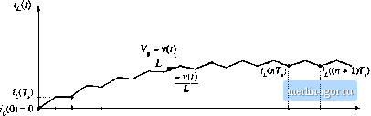 0 dj 7 2Г, Fig. 2.11 Indueior current waveform during convener turn-on irausietit. flows to the output, tlie output capacitor will charge slightly, and v will increase slightly. Tlie process repeats during the second and succeeding switching periods, with the inductor current increasing during each subinterval 1 and decreasing during each subinterval 2. As the output capacitor continues to charge and v increases, the slope during .subinterval 1 decreases while the slope during subinterval 2 becomes more negative. Eventually, the point is reached where the 1псгеа,че in inductor current during subinterval 1 i,4 equal to the decrease in inductor current during subinterval 2. There is then no net change in inductor current over a complete switching period, and the converter operates in steady state. The converter waveforms are periodic: i,(tlTJ) = iiiin + 1)7)-From this point on, the inductor current waveform appears as in Fig. 2.10. The requirement that, in equilibrium, the net change in inductor current over one .switching period be zero lead.s us to ii way to find steady-state conditions in any switching converter: the principle of inductor volt-second balance. Given the definint; relation of an inductor: Integration over one complete .switching period, say from f = 0 to 7j, yields <,(r,)- .(0) = [S,(t}fi( t2.17) (2.18) This equation slates that the net change in inductor current overtme switching period, given by the left-hand side of Eq. (2.18), is proportional to the integral of the applied inductor voltage over the interval. In steady state, the initial and final values of the inductor current are equal, and hence the left-hand side of Eq. (2. IS) is zero. Therefore, in steady state the integral of the applied inductor voltage must be zero: (2.19) The right-hand side of Eq. (2.19) has the units of volt-setonds or flux-linkages. Equation (2.19) states that the total area, or net volt-second.s, under ihe Vfji) waveform must be zero. An equivalent form is obtained by dividing both .sides of Eq. (2.19) by the switching period The right-hand side ofEq. (2.20) is recognized as the average value, twdc component, of v;((j. Etjuation 2.2 liiduaor Voh-Secoiid Balance, Capaciwr Charge Balance, and the Small-Ripple Appro.i:iiiia!ioii Fig, 2.12 The principle of inductor volt-second balance: in steady state, tire net volt-seconds applied to an inductor (i.e., the total area Л) must be zero.
(2.20) states that, in equilibrjiim, the applied inductor voltage must have zero dc component. The inductor voltage waveform of Fig. 2.9 is reproduced in Fig. 2.12, with the area under the V;(0 curve specifically identified. The total area Я is given by the areas of the two rectangles, or The average value is therefore By equating {v,) to zero, and noting that D-) D= l,one obtains ti = dv-{d + d)v = dv-v Solution for V yields (2.21) (2.22) (2.23) (2,24) which coincides with the result obtained previously, Eq. (2.3). So the principle of inductor volt-second balance allows us to derive an expression for the dc component of the converter output voltage. An advantage of this approach is its generality-it can be applied to any converter. One simply sketches the applied mductor voltage waveform, and equates the average value to zero. This method is used later in this chapter, to solve several more complicated converters. Similar arguments can be applied to capacitors. The defining equation of a capacitor is Integration of this equation over one switching period yields (2.25) (2.26) In steady state, the net change over one switching period of the capacitor voltage must be zero, so that the left-hand side of Eq. (2.26) is equal to zero. Therefore, in equilibrium the integral of the capacitor current over one switching period (having the dimensions of amp-seconds, or charge) should be zero. There is no net change in capacitor charge in steady state. An equivalent statement is |