
|
| |
|
Строительный блокнот Introduction to electronics 226 AC Ei/uivalent Circuit Modtliiig !d{i)(T) С Ф HO к R 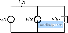 Fig. 7.34 Circuits equivalent tf) the small-signiil converter equations: (n) inductor loop, (b) capacitor node, (c) input pni-t. V +V -7ff 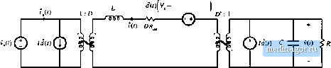 Fig. 735 Complete small-signal uc equivalent circuit model, ttonideal buck-boost converter exatnple. lA CIRCUIT AVERA(iIN(i AND AVERAGED SWITCH MODELIN(i Circuit averaging is another well-known technique for derivation of converter equivalent circuits. Rather than averaging the converter state equations, with the circuit averaging technique we average the converter waveforms directly. All tnanipulation.s are performed on the circuit diagram, instead of on its ec]ua- , dKt) titms, and lieiite the tirtiiit averaging technique gives a more piiysieal interpretatimi to tiie mtwiel. Since circuit averaging involves averaging and small-signal linearization, it is equivalent to state-space averaging. However, in tnany cases circuit averaging is easier to apply, and allows the small-.iiglial ac tnodcl to be written almost by inspection. The circuit averaging technique can also be applied directly to a number of different types of converters and sv/itch elements, including phiLse-controUed rectifiers, PWIVl converters operated in discontinuous conduction mode or with current programming, and quasi-resonant converters-these are described in later chapters. However, in other ca.4es it may lead to involuted models that are less easy to analyze and understand. To overcome this problem, the circuit averaging and state-space averaging approaches can be combined. Circuit averaging was developed before state-space averaging, and is described in [4]. Because of its generality, there has been a recent resurgence of interest in circuit averaging of switch networks [13-20]. The key step in circuit averaging is to replace the converter switches with voltage and current sDutces, to obtain a time-invariant circuit topology. The waveforms of the voltage and current generators are defined to be identical to the switch wavefonns ofthe original converter. Once a time-invariant circuit netwt)rk is obtained, then the ctmverler waveforms can be averaged over tme switching period to remove the switching harmonics. Any nonlinear elements in the averaged circuit model can then be perturbed and linearized, leading to the small-signal ac model. [n Fig. 7.3Й, the switchitig eletnents are separated from the remainder of the converter. The converter therefore consists of a switch network containing the converter switching elements, and a time-invariant network, containing the reactive and other (emaming elements. Figure 7.36 illustrates the simple case in which there are two single-pole single-throw (SPST) switches; the switches can then be represented using a two-port network, [n more complicated systems containing multiple transistors or diodes, such as in polyphase converters, the switch network may contain more than two ports. Power input © Time-invariant network containing converter reactive elements Viit) - 1,(0 (j(0 v,(0 Switch network Control input Load R < v(0 d{t) Fig. 7.36 A switchlna converter can be viewed as a switch network cniuiccted to a time-invariant network. 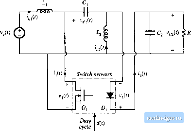 Fig. 7Л7 SdieinLitic of the SEPIC, aminged in the fonn of big. 7.36. The eeiitiai idea of the averaged switch modeling approach is to find an averaged circuit model for the .switch network. The resulting averaged switch model can then be in.4erted into the converter circuit to obtain a complete averaged circuit model of the converter. An important advantage of the averaged switch modeling approach is that the same model can be used in many different converter configurations, [t is not necessary to rederive an averaged circuit model for each particular converter. Furthermore, in many са.чев, the averaged switch model simplifies converter analysis and yields good intuitive understanding of the converter steady-state and dynamic properties. The first step in the process of finding an averaged switch model for a switch network is to sketch the converter in the form of Fig. 7.36, in which a switch network containing only the converter switching elements is explicitly defined. The CCM SEPIC example shown in Fig. 7.37 is used to illustrate the process. There is usually more than one way to define the two ports of the switch network; a natural way to define the two-port switch network of the SEPIC is illustrated in Fig. 7.37. The switch network terminal quantities U[((), f(0. (f). andijO) are illustrated in Fig. 7.38 for CCM operation. Note that it is not necessary that the potts of the switch network be electrically connected within the switch network itself. Furthermore, there is no requirement that any of the terminal voltage or current waveforms of the switch network be nonpulsating. T.4.1 Obtaining a Time-Invariant Circuit The first step in the circuit averaging technique is to replace the switch network with voltage and current sources, such that the circuit connections do not vary in time. The switch network defined in the SEPIC is shown in Fig. 7.39(a). As with any two-port network, two of the four terminal voltages and |