
|
| |
|
Строительный блокнот Introduction to electronics (() Г v,(0 i ,(0 ! v,{0 + Switch network <i()>. ...........---------- d\t){vMT Averaged switch network С: 1 1 Averaged switch network \ Flj . й Dciriviition (if the averaged switch model for llie CCM bt>osi of Hig. 7.45: (a) swjtcli network; (b) .switcli network wheie tho swicclies are replaced by depeiidetit sources whose waveforms match (he switch terminal waveforms; (c) large-signal, nonlineai- averaged swiich model obtained by averaging the switch network lerminal waveforms; (rt) dc and ac small-signal averaged switch network model. 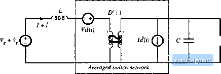 R <v Fig. 7.47 Dc and small-signil at averaged circuit inodel of the boost converter. The tenn lJ(t} is driven by the control input J(l), and is represented by an independent current source. The tenn D(l + i(fi) is dependent on the inductor current (/+ Ht)). This temi is modeled by a dependent current source; this source will become the secondary winding of an ide;il transforiner. Upon elimination of the nonlinear term.s, and replacement of the dependent generators with an ideal !УЛ transfonner, the combined dc and small-signal ac averaged switch model of Fig. 7.46(d) is obtained. Figure 7.47 shows the complete averaged circuit inodel of the boost converter. It is interesting to compare the models of Fig. 7.44(b) and Fig. 7.47. The two averaged circuit mtxJels of the boost converter are equivalent-they result in the same steady-state solution, and the same converter transfer functions. However, since both ports ofthe switch networli in Fig. 7.45(a) share the same reference ground, the resulting averaged circuit model in Fig. 7.47 is easier to solve, and gives better physical insight into steady-state operation and dynamics ofthe boost converter. The circuit imxJel of Fig. 7.47 reveals that the switch network performs the functions of: (i) transformation of dc and small-signal ac voltage and current levels according to the D:l conversion ratio, and (ii) introduction of ac voltage and current variations into the converter circuit, driven by the control input d{t). The model of Fig. 7.47 obtained using the circuit averaging approach is identical to the model of Fig. 7.17(b) obtained using the basic ac modeling technique of Section 7.2. Next, we consider the CCM buck converter of Fig. 7.48, where the switch network ports are defined to share a common ground terminal. The derivation of the corresponding averaged switch nuxJel follows the same steps as in the SEPIC and the boost examples. Let us select V(0 and ijU) as the independent terminal variables ofthe two-port switch network, since these quantities coincide with the applied converter input voltage v(t) and the inductor current ((r), respectively. We then need to express the averaged dependent terminal waveforms snd {vj(0)jj as functions ofthe control input (7(0 and of (v(t)}j. and (ijCO),-- Upon averaging the waveforms of Fig. 7.48(b), one obtains {vj{0}, = f/(0(vi(0},. (7. ISO) Perturbation and linearizadon of Eq. (7.150) then leads to /i + f,(r)=D(/,+;,(r)) + /,(/) (7.151) An equivalent circuit corresponding to Eq. (7.151) is illustrated in Fig. 7.49(.a). Replacement ofthe 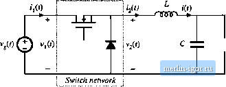 R 4 v(() (,{0 Fig, 7,48 Buck convener example: (a) convener circuit, (b) swiich waveforms. 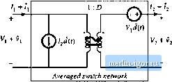 /, + Г, 1 :D o Averaged switch networli Fig. 7.49 Avcrigod switch modcJtiig, buck converter example: (a) tic and small-signal ac avciaged switch model; (b) Averaged circuit model of the buck converiei obtaitied by replacement of the swiich network by the averaged switch model. |
||||||||||||||||||||||||